
A rectifier converts alternating current (AC) into direct current (DC). However, the output of a basic rectifier is not a constant DC voltage. Instead, it contains periodic voltage variations known as ripple.
A full-wave bridge rectifier uses four diodes to convert both halves of an AC waveform into pulsating DC. Adding a smoothing capacitor across the load reduces these voltage variations and produces a significantly more stable DC output.
In this tutorial, we will build and simulate two circuits using SPICE transient analysis:
1. A full-wave bridge rectifier without a filter capacitor.
2. The same rectifier with a parallel smoothing capacitor.
We will examine the output waveforms, measure peak-to-peak ripple voltage, compare first-order textbook approximations with SPICE non-linear diode simulation results, and investigate how capacitance and load resistance affect the output.
You can open and experiment with both interactive circuits directly in your browser:
- Interactive Full-Wave Bridge Rectifier without Filter
- Interactive Full-Wave Bridge Rectifier with 220 µF Filter Capacitor
---
1. How a Full-Wave Bridge Rectifier Works
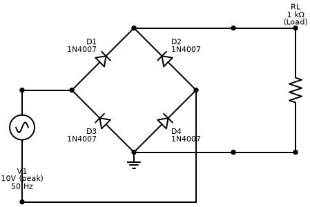
A full-wave bridge rectifier consists of four diodes arranged in a closed loop (the Graetz bridge configuration). The arrangement ensures that current flows through the load in the same direction during both positive and negative half-cycles of the AC input.
Current Flow During Each Half-Cycle
- Positive half-cycle: When node
AC1is more positive than nodeAC2, current flows fromAC1through diodeD1, downward through the load resistorRL, into common ground (0), and returns toAC2through diodeD4. DiodesD2andD3are reverse-biased and block current. - Negative half-cycle: When node
AC2is more positive than nodeAC1, current flows fromAC2through diodeD2, downward through the load resistorRLin the exact same direction, into common ground (0), and returns toAC1through diodeD3. DiodesD1andD4are reverse-biased and block current.
Although the input AC polarity reverses every half-cycle, the current direction through the load remains identical.
Because both half-cycles contribute to the output, the rectified waveform has twice the input AC frequency:
f_ripple = 2 · f_AC
For a 50 Hz AC source, the output ripple frequency is 100 Hz. For a 60 Hz mains supply, it is 120 Hz.
Diode Forward Voltage Drop
During either conducting half-cycle, current passes through two diodes in series (D1 + D4 or D2 + D3). Therefore, the peak output voltage available at the load is approximately:
V_out(peak) ≈ V_in(peak) - 2 · V_D
For standard silicon rectifier diodes such as the 1N4007, the forward voltage drop depends on current and junction temperature. In our simulation, the combined forward drop of the conducting diode pair is approximately 1.45 V.
---
2. Simulating the Rectifier Without a Filter Capacitor
First, let us examine the basic bridge rectifier without a smoothing capacitor.
The simulated circuit uses:
- AC input voltage: 10.0 V peak (20.0 V peak-to-peak)
- Input frequency: 50 Hz
- Four rectifier diodes: 1N4007
- Load resistance: 1 kΩ
Open and simulate the unfiltered bridge rectifier in CircuPilot.
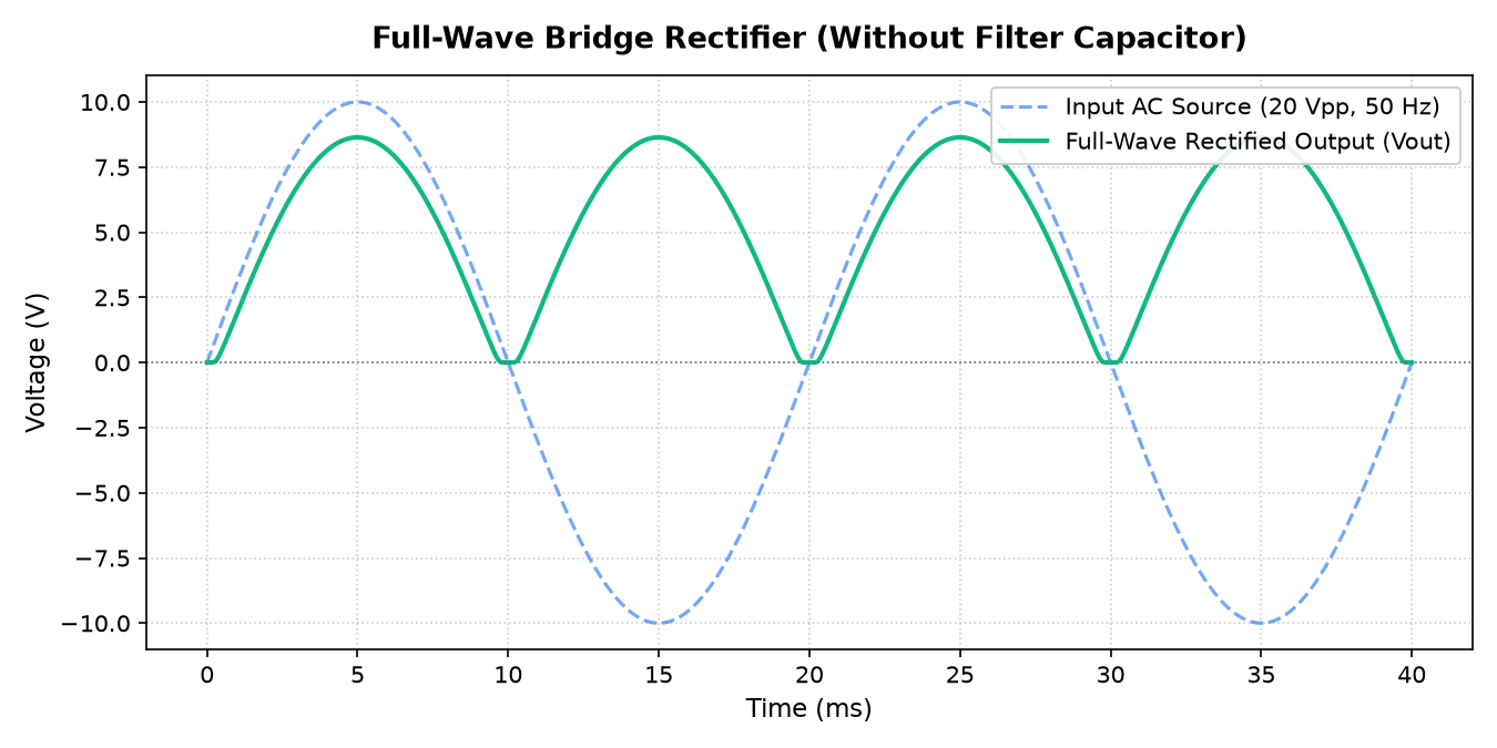
What Does the Simulation Show?
The transient waveform reveals several important circuit characteristics:
1. Both half-cycles become positive: The positive and negative halves of the blue input sine wave produce positive green output pulses across load resistor RL.
2. Peak output voltage: The simulated output reaches approximately 8.55 V, reflecting the combined voltage drop (2 · V_D ≈ 1.45 V) across the two conducting 1N4007 diodes.
3. Dead-zone near zero crossing: When the instantaneous magnitude of the input voltage is less than 2 · V_D (between -1.45 V and +1.45 V), the diodes lack sufficient bias to conduct, and the output drops to 0.0 V.
4. Pulsating DC: The output has a non-zero average DC value, but it repeatedly falls to zero 100 times every second.
For an ideal full-wave rectified sine wave without diode losses, the theoretical average output voltage is:
V_DC = (2 · V_peak) / π ≈ 0.6366 · V_peak
Using the simulated output peak of approximately 8.55 V as a simplified estimate:
V_DC ≈ 0.6366 · 8.55 V ≈ 5.44 V
This is an approximation. The actual average DC value depends on the non-linear diode characteristics and the resulting waveform shape. While this pulsating waveform has a DC average, its continuous swings to zero make it unsuitable as a direct power source for microcontrollers, operational amplifiers, or sensitive digital electronics.
---
3. Adding a Smoothing Capacitor
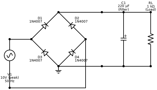
A straightforward way to reduce rectifier ripple is to connect a capacitor in parallel with the load resistor. The capacitor stores electrical energy when the rectified voltage rises and releases that energy into the load when the input voltage falls.
How the Capacitor Works
The charging and discharging process occurs in four distinct phases:
1. Charging: As the rectified input voltage rises above the capacitor voltage, the forward-biased diode pair conducts, charging the capacitor up to V_out(peak).
2. Diode cut-off: After the AC input passes its peak and begins to fall below the capacitor voltage, the diodes become reverse-biased and stop conducting.
3. Discharging: The capacitor acts as an independent energy reservoir, supplying current to load resistor RL while the input voltage remains below the stored capacitor voltage.
4. Recharging: During the next rising half-cycle, the opposite diode pair conducts again and replenishes the capacitor charge.
During the discharge interval, the capacitor voltage approximately follows the exponential RC discharge relationship:
v_out(t) = V_initial · e^(-t / (R_L · C))
Where R_L is the load resistance and C is the filter capacitance.
Open and simulate the capacitor-filtered bridge rectifier in CircuPilot.
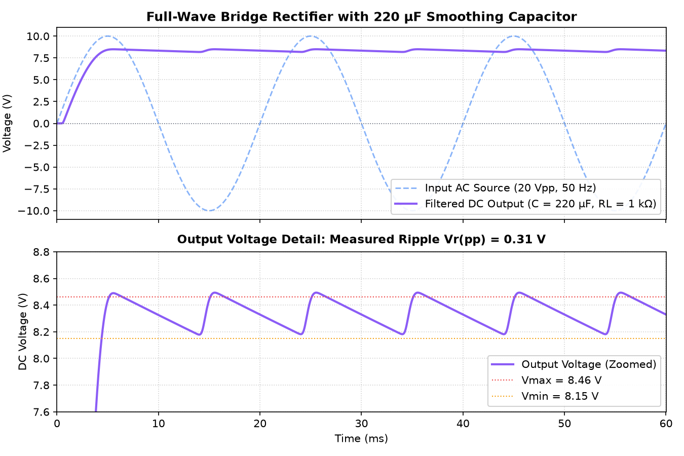
Unlike the unfiltered circuit, the output no longer falls to zero between rectified peaks. Instead, it stays near a steady DC level with a smaller periodic variation called peak-to-peak ripple voltage, written as V_r(pp).
---
4. Understanding Ripple Voltage: Theory vs. SPICE Simulation
A commonly used first-order approximation for the ripple voltage of a full-wave rectifier with a capacitor filter is:
V_r(pp) ≈ I_load / (f_ripple · C)
Since the ripple frequency is twice the AC input frequency:
V_r(pp) ≈ I_load / (2 · f_AC · C)
The average load current can be approximated by Ohm's law:
I_load ≈ V_DC / R_L
Combining these relationships gives:
V_r(pp) ≈ V_DC / (2 · f_AC · R_L · C)
Where:
V_r(pp)is the peak-to-peak ripple voltage.I_loadis the average load current.f_ACis the AC input frequency (50 Hz).Cis the filter capacitance in Farads.R_Lis the load resistance in Ohms.V_DCis the average DC output voltage.
This formula is useful for initial design estimates, but it is not an exact prediction for every real circuit. It assumes a simplified linear discharge over the entire half-period and is most accurate when the ripple is relatively small.
Worked Example: 220 µF Capacitor and 1 kΩ Load
For our simulated circuit:
- AC input frequency: 50 Hz
- Ripple frequency: 100 Hz
- Filter capacitance: 220 µF
- Load resistance: 1 kΩ
- Approximate average DC output: 8.35 V
The average load current is approximately:
I_load ≈ 8.35 V / 1000 Ω = 8.35 mA
The theoretical first-order ripple estimate is:
V_r(pp) ≈ 0.00835 A / (100 Hz · 220 × 10⁻⁶ F) ≈ 0.379 V
Comparing the Calculation with SPICE Simulation
The SPICE transient simulation using non-linear 1N4007 diode models yields the following measurements:
| Measurement | SPICE Simulation Result |
|---|---|
| Maximum output voltage (V_max) | 8.46 V |
| Minimum output voltage (V_min) | 8.15 V |
| Peak-to-peak ripple (V_r(pp)) | 0.311 V |
| Average DC output (V_DC) | 8.34 V |
The simulated ripple (0.311 V) is approximately 18% lower than the first-order estimate (0.379 V).
Why Are the Two Results Different?
1. The capacitor does not discharge for the entire half-cycle: The simplified textbook formula assumes discharge occurs over the complete 10 ms half-period (T / 2). In the simulated circuit, the diodes begin conducting before the trough reaches 10 ms, replenishing charge during a conduction window of roughly 1.5 ms to 2.0 ms. This leaves only about 8.0 ms for discharge. Because the discharge interval is shorter, the capacitor loses less voltage.
2. Capacitor discharge is exponential, not linear: The voltage follows an exponential decay curve (e^(-t / RC)), which flattens out as voltage decreases, rather than an idealized linear ramp.
3. Diode non-linearities and dynamic impedance: The non-linear forward characteristics, series resistance (Rs), and junction capacitance of the 1N4007 model influence the charging current pulses and peak crest shape.
This comparison provides an instructive engineering takeaway: textbook formulas provide simplified first-order estimates, while transient SPICE simulation captures the detailed physical dynamics of the specific component models and operating conditions.
---
5. Experiment: How Capacitance Affects Ripple Voltage
What happens when we increase the filter capacitor?
To investigate, we keep the AC input at 10.0 V peak and 50 Hz, and load resistance at 1 kΩ. We then sweep capacitance across standard values from 10 µF to 1000 µF.
The following values were measured in SPICE simulation:
| Capacitance (C) | V_max (V) | V_min (V) | Simulated Ripple (V) | Theoretical Ripple (V) | Average V_DC (V) |
|---|---|---|---|---|---|
| 10 µF | 8.63 V | 4.59 V | 4.04 V | 6.75 V | 6.75 V |
| 47 µF | 8.59 V | 7.29 V | 1.30 V | 1.70 V | 7.96 V |
| 100 µF | 8.53 V | 7.87 V | 0.66 V | 0.82 V | 8.21 V |
| 220 µF | 8.46 V | 8.15 V | 0.31 V | 0.38 V | 8.34 V |
| 470 µF | 8.41 V | 8.26 V | 0.15 V | 0.18 V | 8.35 V |
| 1000 µF | 8.37 V | 8.30 V | 0.07 V | 0.08 V | 8.35 V |
What Can We Learn from the Capacitance Sweep?
1. Larger capacitance reduces ripple: Increasing capacitance stores more charge, holding the output voltage higher between successive charging pulses. Increasing capacitance from 100 µF to 1000 µF reduces ripple from approximately 0.66 V down to 0.07 V.
2. The theoretical approximation improves with larger capacitance: For small capacitors (10 µF), ripple is large and the discharge interval is long, so the small-ripple linear approximation overestimates ripple. At larger capacitances (220 µF to 1000 µF), the small-ripple assumption holds and the formula closely tracks the SPICE simulation.
3. The maximum peak voltage shifts slightly: Notice that V_max decreases slightly as capacitance increases (from 8.63 V with 10 µF to 8.37 V with 1000 µF). Larger capacitors demand higher surge current pulses during shorter conduction intervals, causing an increased forward voltage drop across the diode internal resistance.
A larger capacitor reduces voltage ripple, but it also alters the current pulses drawn during recharging. Practical capacitor selection must balance ripple reduction against diode current stress and capacitor physical volume.
---
6. Experiment: How Load Resistance Affects Ripple Voltage
Capacitance is not the only factor that determines ripple; load resistance also has a major effect. A lower load resistance draws more current from the capacitor, causing it to discharge more rapidly between charging pulses.
For this experiment, we keep the capacitor fixed at 220 µF and sweep the load resistance RL.
| Load Resistance (RL) | Load Current (I_load) | V_max (V) | V_min (V) | Simulated Ripple (V) | Theoretical Ripple (V) |
|---|---|---|---|---|---|
| 470 Ω | 17.3 mA | 8.42 V | 7.79 V | 0.62 V | 0.78 V |
| 1 kΩ | 8.3 mA | 8.46 V | 8.15 V | 0.31 V | 0.38 V |
| 2.2 kΩ | 3.8 mA | 8.51 V | 8.37 V | 0.14 V | 0.17 V |
| 4.7 kΩ | 1.8 mA | 8.57 V | 8.50 V | 0.07 V | 0.08 V |
Engineering Insights from the Load Sweep
1. Heavier loads increase ripple: When load resistance decreases (e.g. 470 Ω drawing 17.3 mA), the capacitor discharges much faster during the diode cut-off interval, approximately doubling the ripple compared to a 1 kΩ load.
2. Lighter loads produce a smoother output: At 4.7 kΩ, the load current is only 1.8 mA and the measured ripple is approximately 70 mV.
3. Always design for worst-case maximum load: A DC power supply must always be sized for its maximum anticipated load current. A capacitor filter that produces acceptable 50 mV ripple under light standby load may permit unacceptable 1.0 V ripple when the connected system draws full operating power.
---
7. Practical Design Considerations
While a capacitor-filtered bridge rectifier is simple to model, practical hardware design requires attention to component ratings, thermal conditions, and operating environments:
1. Capacitor voltage rating: Select an electrolytic capacitor with a working voltage rating comfortably above the maximum expected DC voltage. Account for AC mains line tolerance (e.g. +10%), no-load transformer voltage rise, and potential line transients. For example, a 16 V or 25 V capacitor is often appropriate for a 10 V peak output, but the final choice must be evaluated against the circuit worst-case peak voltage.
2. Electrolytic capacitor polarity: Connect the positive terminal to the positive DC output rail and the negative terminal to ground. Reversing the polarity of an electrolytic capacitor will cause overheating, electrolyte leakage, or catastrophic casing rupture.
3. Diode peak inverse voltage (PIV): In a bridge rectifier, each reverse-biased diode must withstand the maximum peak reverse voltage developed across the bridge circuit: PIV ≥ V_in(peak). The 1N4007 is rated for a maximum repetitive peak reverse voltage of 1000 V; however, component selection should always be verified against the transformer secondary voltage, load characteristics, and potential line transients rather than reverse voltage ratings alone.
4. Diode current ratings and thermal limits: Check the average forward current (I_F(AV)), repetitive peak forward current (I_FRM), non-repetitive surge rating (I_FSM), and thermal dissipation. Charging a large filter capacitor draws current in short, high-amplitude pulses during each half-cycle. A diode suitability cannot be determined from average DC load current alone.
5. Transformer secondary resistance: Ideal SPICE voltage sources have zero internal resistance. Real step-down transformers possess secondary winding resistance and leakage inductance that limit surge currents but also cause the output voltage to sag under heavy load. Incorporating realistic source resistance improves simulation accuracy.
6. Filtering is not voltage regulation: A smoothing capacitor reduces AC ripple, but it does not regulate DC output voltage. Fluctuations in AC mains voltage or changes in load current will cause the average DC output to drift. When a stable, noise-immune supply rail is required for sensitive analog or digital circuits, the filtered output should feed an active linear regulator (such as an LM7805 or LM317) or a switching DC-DC converter.
7. Electrical safety: Always use an isolated, low-voltage AC step-down transformer or benchtop AC signal generator for physical experiments. Never connect a breadboard rectifier circuit directly to 120 V or 230 V mains electricity.
---
8. Conclusion & Next Steps
A full-wave bridge rectifier with a smoothing capacitor is an essential building block of AC-to-DC power conversion:
- Four bridge diodes rectify both halves of the AC waveform, doubling the ripple frequency to
2 · f_AC(100 Hz for 50 Hz lines). - Two diode forward drops (
≈ 1.45 Vtotal for 1N4007) reduce the available peak DC voltage below the AC input peak. - A parallel capacitor acts as an energy reservoir, storing charge during voltage peaks and discharging into the load when the input voltage drops.
- Ripple voltage is inversely proportional to capacitance and load resistance:
V_r(pp) ≈ I_load / (2 · f_AC · C). - In this particular simulation, the measured ripple was approximately 15% to 20% lower than the first-order estimate due to finite diode conduction time and exponential discharge dynamics.
Explore the Interactive Circuits
You can explore both circuits, adjust component values, and test different filter capacitors directly in CircuPilot:
- Launch Full-Wave Bridge Rectifier without Filter
- Launch Full-Wave Bridge Rectifier with 220 µF Capacitor
Frequently asked questions
Why does a full-wave rectifier produce twice the input AC frequency?
During each full cycle of the input AC sine wave, current flows through the load in the same direction during both the positive and negative half-cycles. A 50 Hz AC input produces 100 rectified pulses per second, making the fundamental ripple frequency 100 Hz (120 Hz for 60 Hz lines).
Why does SPICE simulation report less ripple than the textbook formula Vr(pp) ≈ Iload / (2 · f · C)?
The textbook formula is a first-order approximation that assumes linear discharge over the entire half-period (T/2). In reality, the rectifier diodes conduct during a non-zero charging interval (the conduction angle), meaning the capacitor only discharges for a fraction of the half-cycle. Furthermore, the discharge is exponential rather than linear.
How does increasing filter capacitance affect diode stress?
While a larger capacitor reduces voltage ripple, it forces the diodes to replenish the stored charge in much shorter, higher-current bursts. Designers must check repetitive peak forward current (IFRM), surge ratings (IFSM), and thermal limits rather than average load current alone.
Does adding a smoothing capacitor provide voltage regulation?
No. A smoothing capacitor reduces AC ripple, but the average DC output voltage will still sag as the load current increases or if the AC line voltage fluctuates. Regulating the output requires an active linear regulator (such as an LM7805 or LM317) or a switching DC-DC converter.
How should the working voltage rating (WVDC) of the filter capacitor be chosen?
The capacitor rated working voltage must comfortably exceed the peak DC output under no-load conditions, accounting for high AC line tolerance (e.g. +10%) and transformer secondary regulation. Operating too close to rated voltage accelerates electrolyte drying and premature failure.