
The inverting amplifier is one of the most widely used fundamental building blocks in analog electronics. By directing a portion of the output signal back to the inverting input (V−) through a negative feedback resistor (Rf), the circuit establishes stable, predictable voltage amplification that is governed by the ratio of two passive resistors.
In this comprehensive guide, you will explore the circuit architecture of an inverting amplifier built around the industry-standard LM741 operational amplifier, walk through the step-by-step mathematical derivation of its closed-loop gain, understand the physical reality of the virtual ground, analyze what happens when the output transistors clip against the power supply rails, and verify every operating point using interactive SPICE simulation directly in your browser.
⚡ Test this Op-Amp Circuit in Your Browser
You can launch and test this verified pre-wired LM741 inverting amplifier with live digital voltmeters and real ngspice simulation on CircuPilot — no software installation or sign-up required:
---
1. Circuit Schematic and Operational Principles
An inverting amplifier consists of an operational amplifier, an input resistor (Rin), a negative feedback resistor (Rf), a load resistor (RL), and a dual (split) DC power supply (+Vcc and −Vee):
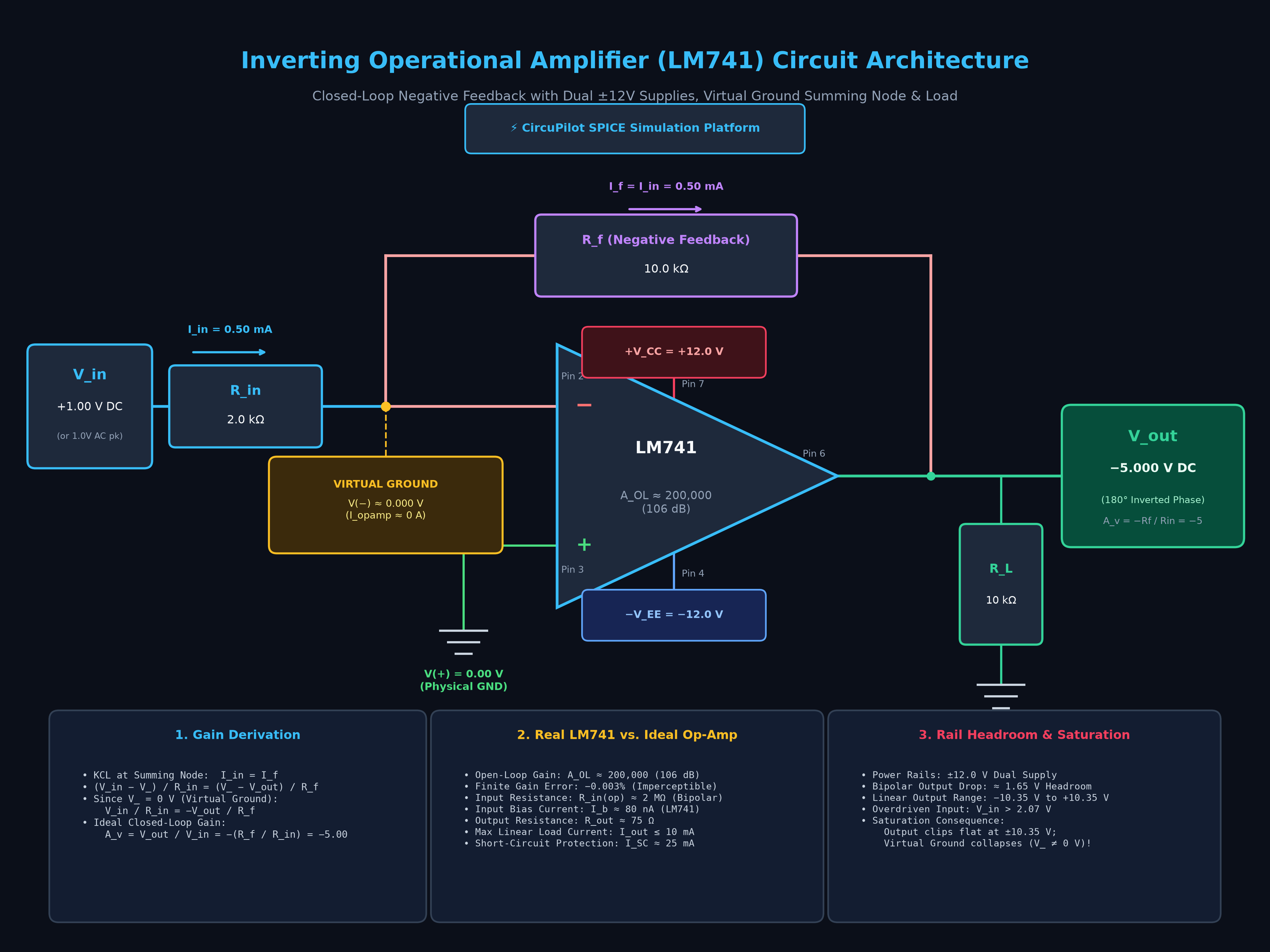
Figure 1: Complete schematic diagram of the inverting operational amplifier circuit with negative feedback, virtual ground summing node, and dual ±12V power rails. Verified and simulated in CircuPilot.
The Ideal Op-Amp Assumptions
To analyze the circuit, circuit designers frequently apply two classical operational amplifier approximations:
1. Infinite Input Impedance (Rin(op) → ∞): The internal input stages draw negligible current (I+ = I− ≈ 0 A).
2. Infinite Open-Loop Gain (AOL → ∞): With negative feedback present, the amplifier continuously drives its output terminal to force the differential input voltage (V+ − V−) toward zero.
The Virtual Ground Concept
In this inverting topology, the non-inverting terminal (V+, Pin 3) is connected directly to circuit ground (0.00 V). Under negative feedback, the op-amp continuously adjusts its output voltage until:
V− ≈ V+ = 0.00 V
Although the inverting node (V−, Pin 2) is not physically wired to ground, its potential is clamped at zero volts by the feedback loop. This node is known as a virtual ground.
Because V− sits at zero volts, the input signal source only sees the series resistance Rin between itself and the virtual ground. Therefore, the input impedance of the inverting amplifier circuit is exactly equal to Rin:
Zin = Rin
---
2. Deriving the Inverting Closed-Loop Gain Formula
Applying Kirchhoff's Current Law (KCL) at the inverting summing node (V−):
Iin = If + I−
Because an ideal op-amp draws no input current (I− = 0):
Iin = If
Now express each current in terms of nodal voltages using Ohm's law:
Iin = (Vin − V−) / Rin = (Vin − 0) / Rin = Vin / Rin
If = (V− − Vout) / Rf = (0 − Vout) / Rf = −Vout / Rf
Equating the two currents:
Vin / Rin = −Vout / Rf
Rearranging to solve for the closed-loop voltage gain (Av):
Av = Vout / Vin = −(Rf / Rin)
Vout = −(Rf / Rin) · Vin
The Physical Meaning of the Negative Sign
The negative sign signifies a 180° phase inversion:
- A positive DC input voltage (
+1.00 V) forces the output to swing negative (−5.00 V). - A negative DC input voltage (
−1.00 V) forces the output to swing positive (+5.00 V). - An AC sinusoidal input signal produces an inverted AC output waveform whose peaks and troughs are mirrored across the zero-volt axis.
Real Op-Amp Correction: Accounting for Finite Open-Loop Gain
In practical engineering, no physical op-amp has infinite open-loop gain. The LM741 has a typical DC open-loop gain of AOL ≈ 200,000 (approximately 106 dB).
The exact closed-loop gain formula accounting for finite AOL is:
Av(real) = −(Rf / Rin) / [1 + (1 + Rf / Rin) / AOL]
For our target design with Rin = 2 kΩ, Rf = 10 kΩ (ideal gain −5.00), and AOL = 200,000:
Av(real) = −5.00 / [1 + (1 + 5) / 200,000] = −5.00 / [1 + 0.00003] = −4.99985 V/V
The finite gain error is only −0.003%, which is completely negligible compared to the 1% or 5% tolerance of standard physical resistors. Thus, within its linear operating boundaries, the closed-loop gain is governed almost entirely by the passive resistor ratio.
---
3. Practical Circuit Design: Av = −5.00 V/V on Dual ±12V Supplies
Let us design a practical inverting amplifier circuit with a voltage gain of −5.00 V/V powered by standard dual ±12.0 V DC supplies using an LM741 operational amplifier.
Step 1: Selecting the Input Resistor (Rin = 2 kΩ)
The choice of Rin determines the input impedance of the amplifier:
- If Rin is chosen too small (e.g., 100 Ω): The circuit draws substantial input current (
10 mAat1 V), heavily loading and attenuating preceding high-impedance signal sources or sensor outputs. - If Rin is chosen too large (e.g., 500 kΩ): Achieving a gain of 5 requires an
Rfof2.5 MΩ. Very high resistor values significantly increase Johnson-Nyquist thermal noise (Vn = √(4 · kB · T · R · Δf)), make the summing node vulnerable to stray parasitic PCB capacitance, and induce significant DC offset voltages from the LM741's input bias current (Ib ≈ 80 nAtypical). - The Engineering Compromise: Selecting
Rin = 2.0 kΩprovides an input impedance that typical signal sources can comfortably drive, keeps Johnson thermal noise minimal, and maintains reasonable resistor sizing.
Step 2: Calculating the Feedback Resistor (Rf = 10 kΩ)
With Rin = 2.0 kΩ and desired gain |Av| = 5.00:
Rf = |Av| · Rin = 5.00 · 2.0 kΩ = 10.0 kΩ
Both 2.0 kΩ and 10.0 kΩ are standard E24 resistor values.
Step 3: Load Resistor and Output Current Verification
We place a standard 10 kΩ load resistor (RL) at the output terminal. When the output delivers Vout = −5.00 V:
- Current through the feedback resistor:
If = 5.00 V / 10 kΩ = 0.50 mA - Current through the load resistor:
IL = 5.00 V / 10 kΩ = 0.50 mA - Total op-amp output current:
Iout = If + IL = 1.00 mA
According to the LM741 datasheet:
- Maximum Recommended Linear Output Current:
5 mA to 10 mA(or load resistanceRL ≥ 2 kΩ). Our1.00 mAoperating current operates well within this linear window, ensuring minimal internal heating and distortion. - Short-Circuit Protection Limit:
ISC ≈ 25 mAtypical. This is an emergency internal protection limit that prevents device destruction during an accidental dead short to ground; it is not a rated continuous linear operating current.
---
4. SPICE-Verified DC Operating Point Analysis
To verify theoretical calculations against real physical transistor models, we simulate the complete circuit using CircuPilot's ngspice simulation engine.
The table below records the theoretical linear target, simulated output voltage (Vout), the voltage at the inverting summing node (V−), and the physical operating state across a range of DC input voltages:
| DC Input (Vin) | Ideal Target Vout | SPICE Simulated Vout | Inverting Node V(−) | Operating State |
|---|---|---|---|---|
| +0.10 V | −0.50 V | −0.5000 V | +0.0000 V (2.8 µV) | Linear Amplification |
| +0.50 V | −2.50 V | −2.4999 V | +0.0000 V (13.8 µV) | Linear Amplification |
| +1.00 V | −5.00 V | −4.9998 V | +0.0000 V (27.7 µV) | Linear Amplification |
| +1.50 V | −7.50 V | −7.4997 V | +0.0000 V (41.5 µV) | Linear Amplification |
| +2.00 V | −10.00 V | −9.9994 V | +0.0001 V (55.4 µV) | Linear (Near Negative Rail) |
| +2.10 V | −10.50 V | −10.3446 V | +0.0259 V (25.9 mV) | Negative Output Saturation |
| +2.50 V | −12.50 V | −10.3422 V | +0.3596 V (360 mV) | Negative Output Saturation |
| +3.00 V | −15.00 V | −10.3391 V | +0.7768 V (777 mV) | Negative Output Saturation |
| −0.50 V | +2.50 V | +2.4999 V | −0.0000 V (−13.8 µV) | Linear Amplification |
| −1.00 V | +5.00 V | +4.9998 V | −0.0000 V (−27.7 µV) | Linear Amplification |
| −2.00 V | +10.00 V | +9.9994 V | −0.0001 V (−55.4 µV) | Linear (Near Positive Rail) |
| −3.00 V | +15.00 V | +10.3391 V | −0.7768 V (−777 mV) | Positive Output Saturation |
The Mechanism of Output Saturation and Virtual Ground Collapse
Notice the dramatic shift that occurs when Vin exceeds +2.07 V:
1. Headroom Limitation: On a dual ±12.0 V power supply, the internal bipolar output transistors (emitter followers and current limit resistors) require approximately 1.5 V to 1.7 V of internal drop. Consequently, the maximum achievable linear output voltage swings between +10.35 V and −10.35 V. This ±10.35 V boundary is specific to our ±12 V rails, 10 kΩ load, and the SPICE macromodel parameters; on ±15 V rails, saturation would occur near ±13.5 V.
2. The Feedback Resistor Remains Connected: During saturation, the physical feedback resistor Rf does not break or disconnect.
3. Loss of Equilibrium: The op-amp output driver reaches its physical limit at −10.35 V and cannot swing any further negative. As a result, it can no longer pull sufficient current through Rf to counteract the incoming current Iin = Vin / Rin.
4. Virtual Ground Collapse: Because the output cannot supply the necessary balancing voltage, negative feedback fails to maintain V− = V+. At Vin = +3.00 V, the summing junction voltage V− climbs to +0.777 V, clearly demonstrating the complete breakdown of the virtual ground condition.
---
5. AC Transient Waveform Analysis (1 kHz Sine Wave)
To observe dynamic behavior, phase relationships, and clipping, we drive the amplifier with a 1 kHz sinusoidal signal under two distinct operating conditions:
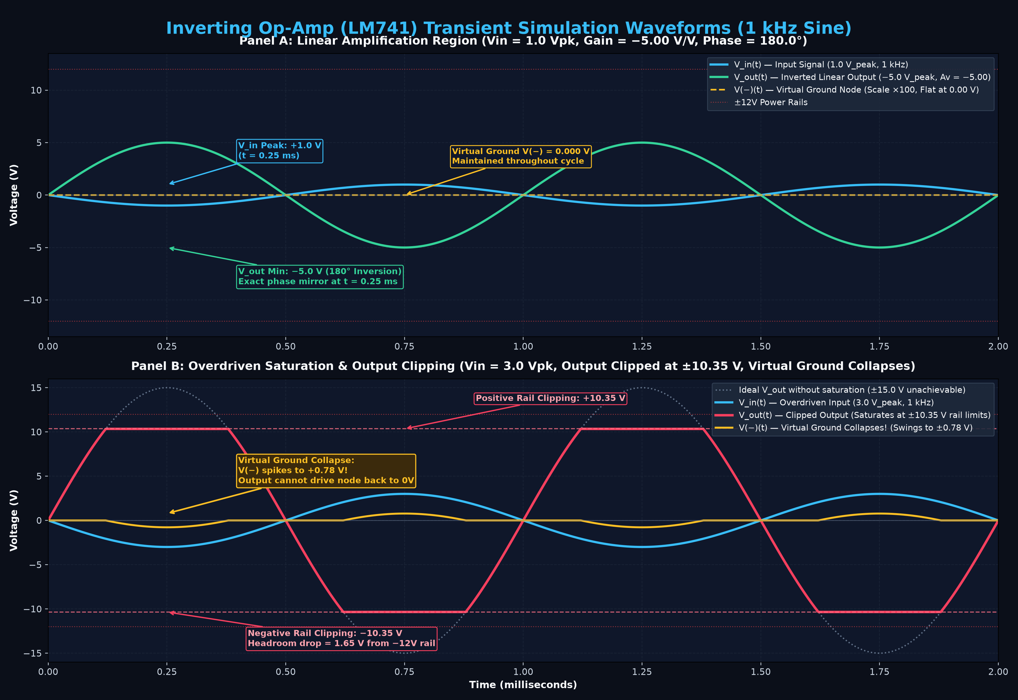
Panel A: Linear Operation (Vin = 1.0 Vpk, 2.0 Vp-p)
- Input Signal:
Vin(t) = 1.0 · sin(2π · 1000 · t) V - Output Signal:
Vout(t) = −5.0 · sin(2π · 1000 · t) V(a clean10.0 Vp-psine wave). - Phase Shift: When
Vinreaches its positive crest of+1.000 Vatt = 0.25 ms,Voutsimultaneously reaches its negative trough of−4.9998 V. Transient analysis measures a phase shift of 180.0° (within numerical simulation resolution), confirming ideal signal inversion. - Virtual Ground Stability: As shown by the amber trace in Panel A, node
V−(t)remains firmly anchored at0.00 V(under30 µVripple) throughout the entire AC cycle.
Panel B: Overdriven Operation & Output Clipping (Vin = 3.0 Vpk, 6.0 Vp-p)
- Clipping Behavior: An ideal linear equation predicts that a
3.0 Vpkinput produces a±15.0 Vpkoutput (30 Vp-p). However, as shown by the red trace in Panel B, the output waveform is clipped flat at+10.35 Von positive peaks and−10.35 Von negative peaks. - Waveform Distortion: The output transitions from a pure sine wave into a heavily distorted trapezoidal waveform rich in odd harmonics.
- Summing Node Spikes: In Panel B, whenever
Voutclips against either rail, nodeV−(t)immediately spikes to+0.78 Vand−0.78 V. As soon as the input wave drops back into the linear window (|Vin| < 2.07 V), the op-amp recovers from saturation, and the virtual ground immediately snaps back to0.00 V.
---
6. Inverting vs. Non-Inverting Op-Amp Topologies
When selecting an operational amplifier configuration for your design, consider the distinct electrical trade-offs between the inverting and non-inverting configurations:
| Parameter | Inverting Amplifier | Non-Inverting Amplifier |
|---|---|---|
| Gain Formula | Av = −Rf / Rin | Av = 1 + (Rf / Rin) |
| Gain Range | 0 to −∞ (Can attenuate if Rf < Rin) | ≥ 1 (Cannot attenuate signals) |
| Phase Relationship | Inverted (180° phase shift) | Non-inverted (0° phase shift) |
| Input Impedance (Circuit) | Moderate: Equal to Rin (typically 1 kΩ to 50 kΩ) | Extremely high: Equal to op-amp common-mode input resistance |
| Op-Amp Input Stage | Summing node is held at Virtual Ground (0 V) | Both input terminals track the input voltage Vin |
| Common-Mode Distortion | Virtually Zero: Input pins never experience voltage swings | Subject to common-mode voltage swings and CMRR limits |
| LM741 Device Input Impedance | 0.3 MΩ to 2 MΩ (Bipolar input differential pair) | 0.3 MΩ to 2 MΩ (LM741) vs. > 1 GΩ (Modern FET-input op-amps) |
Notice the crucial difference in input impedance: In an inverting amplifier, circuit input impedance is determined by
Rin, not the op-amp chip. In a non-inverting amplifier, the input signal connects directly to the op-amp's non-inverting terminal (V+), yielding input impedances of10^12 Ωwith modern FET-input op-amps (such as TL071 or OPA134), but0.3 MΩ to 2 MΩwhen using a classic bipolar LM741.
---
7. Common Design Traps & Engineering Checklist
1. The Missing Feedback Resistor (Open-Loop Trap)
If Rf is accidentally omitted or disconnected, the circuit loses negative feedback. The op-amp reverts to its raw open-loop gain (AOL ≈ 200,000). Even a microvolt of input offset voltage drives the output into hard saturation against either the +10.35 V or −10.35 V rail, turning the amplifier into an accidental comparator.
2. Single-Supply Biasing Mistakes
The LM741 was specifically designed for split (dual) power supplies. If you power an LM741 with a single +12.0 V supply (Vcc = +12 V, Vee = 0 V / GND):
- Input Common-Mode Range Violation: The LM741's input stage requires signals to stay at least
2.0 V to 3.0 Vaway from both supply rails (Vee + 2 V ≤ Vcm ≤ Vcc − 2 V). Tying the non-inverting terminal (Pin 3) directly to0 Vviolates this requirement. - Output Swing Limitation: The LM741's output cannot swing down to
0 V; it typically saturates at+1.5 V to +2.0 Vabove ground. - The Correct Single-Supply Solution: To operate on a single supply, you must create an artificial virtual ground at mid-supply (
Vcc / 2 = +6.0 V) using a two-resistor voltage divider, biasPin 3to this+6 Vreference, and place AC coupling capacitors at the input and output to block DC current.
3. Confusing Short-Circuit Current with Linear Drive
Datasheets specify an output short-circuit current (ISC ≈ 25 mA) for the LM741. This rating indicates the maximum current the internal protection circuit allows before current limiting kicks in during a dead short. It does not mean you can drive a low-impedance load (like an 8 Ω speaker or 50 Ω cable) linearly. For linear amplification with minimal distortion, keep total output current (IL + If) under 10 mA (loads RL ≥ 2 kΩ).
4. Excessive Resistor Sizing
Avoid using resistor values below 1 kΩ (which demand excessive output current and cause distortion) or values above 100 kΩ with bipolar op-amps like the LM741 (where input bias current Ib ≈ 80 nA flowing through a large resistor creates measurable DC offset voltages at the output).
---
8. Interactive SPICE Experimentation in CircuPilot
CircuPilot allows you to simulate and probe this inverting amplifier interactively in your browser without installing software.
The pre-wired circuit is configured with live digital voltmeters monitoring three key nodes:
1. VM_IN: Monitors the applied input voltage (Vin = +1.000 V).
2. VM_NEG: Probes the inverting summing node (V−), confirming the virtual ground reading of 27.7 µV (0.000 V).
3. VM_OUT: Monitors the amplified output voltage (Vout = −5.000 V).
Experiments to Try in the Browser:
1. Verify Linearity: Click the input voltage source V_IN, edit its value from 1 V to 1.5 V, and press Run. Notice that VM_OUT updates to -7.500 V while VM_NEG remains anchored at 0.000 V.
2. Observe Output Saturation: Change V_IN to 3.0 V and run the simulation. Watch VM_OUT clamp at -10.339 V (rail limit) and observe VM_NEG spike to +0.777 V, visually demonstrating the collapse of the virtual ground.
3. Inversion with Negative Input: Change V_IN to -1.0 V. Observe VM_OUT rise to +4.9998 V (positive output from negative input).
4. Change Closed-Loop Gain: Change R_F from 10k to 20k to achieve Av = -10.0 V/V, or change R_F to 2k for unity gain (Av = -1.0 V/V).
⚡ Run and Modify the Circuit Live
Click the link below to open the complete, verified LM741 inverting amplifier on the CircuPilot canvas. Press Run to simulate immediately, or adjust component values on the fly:
---
Frequently Asked Questions (FAQ)
What is an inverting operational amplifier?
An inverting operational amplifier is a closed-loop linear analog circuit where the input signal is applied through an input resistor (Rin) to the op-amp's inverting terminal (−), while the non-inverting terminal (+) is connected to circuit ground. Negative feedback provided by a feedback resistor (Rf) stabilizes the closed-loop voltage gain at Av = −Rf / Rin and produces an output that is 180° out of phase with the input.
What is a virtual ground in an op-amp circuit?
A virtual ground is a circuit node that is held at approximately zero volts without being physically connected to the ground reference. Because the non-inverting terminal is tied to physical ground (0 V) and the op-amp has enormous open-loop gain (typically 200,000 in an LM741), negative feedback continuously drives the output to keep the differential input voltage (V+ − V−) near zero. Thus, the inverting terminal stays at 0.00 V while carrying virtually zero input current into the op-amp.
Why is the closed-loop gain formula negative?
The negative sign in Av = −Rf / Rin signifies a 180-degree phase inversion. Because the non-inverting terminal is fixed at 0 V, a positive increase in input voltage causes input current to flow toward the summing node; to pull this node back to 0 V, the op-amp output must swing negative. Conversely, a negative input voltage forces the output to swing positive.
What happens to the virtual ground when an op-amp saturates?
During output saturation or rail clipping, the internal output transistors reach their voltage drop limits (typically 1.5 V to 2 V away from the supply rails in a bipolar op-amp like the LM741). Because the output cannot swing any further to supply the balance current required through Rf, the negative feedback loop can no longer maintain equilibrium. As a result, the virtual ground collapses, and the inverting terminal voltage deviates significantly from 0 V.
How do you choose Rin and Rf for an inverting amplifier?
Selecting Rin and Rf is an engineering tradeoff between input loading, Johnson-Nyquist thermal noise, and op-amp output drive capability. Because the input impedance of an inverting amplifier equals Rin, choosing Rin too small (e.g., 100 Ω) heavily loads the preceding signal source. Choosing Rin too large (e.g., 1 MΩ) requires a massive Rf, increasing thermal noise, stray capacitance, and DC offset errors from input bias currents. Standard values between 1 kΩ and 50 kΩ (such as Rin = 2 kΩ and Rf = 10 kΩ for a gain of −5) represent an optimal balance.
Can an LM741 operate on a single positive power supply?
An LM741 can operate on a single supply (such as +12 V and 0 V) only if the non-inverting input is biased to an artificial mid-supply virtual ground (Vcc / 2 = +6 V) using a resistive voltage divider and AC coupling capacitors are added to the input and output. Because the LM741's input common-mode voltage range requires inputs to stay at least 2 V to 3 V away from both supply rails and its output cannot swing down to 0 V, connecting the non-inverting terminal directly to 0 V on a single supply causes immediate output clipping and operational failure.
Frequently asked questions
What is an inverting operational amplifier?
An inverting operational amplifier is a closed-loop linear analog circuit where the input signal is applied through an input resistor (Rin) to the op-amp's inverting terminal (-), while the non-inverting terminal (+) is connected to circuit ground. Negative feedback provided by a feedback resistor (Rf) stabilizes the closed-loop voltage gain at Av = -Rf / Rin and produces an output that is 180 degrees out of phase with the input.
What is a virtual ground in an op-amp circuit?
A virtual ground is a circuit node that is held at approximately zero volts without being physically connected to the ground reference. Because the non-inverting terminal is tied to physical ground (0 V) and the op-amp has enormous open-loop gain (typically 200,000 in an LM741), negative feedback continuously drives the output to keep the differential input voltage (V+ - V-) near zero. Thus, the inverting terminal stays at 0.00 V while carrying virtually zero input current into the op-amp.
Why is the closed-loop gain formula negative?
The negative sign in Av = -Rf / Rin signifies a 180-degree phase inversion. Because the non-inverting terminal is fixed at 0 V, a positive increase in input voltage causes input current to flow toward the summing node; to pull this node back to 0 V, the op-amp output must swing negative. Conversely, a negative input voltage forces the output to swing positive.
What happens to the virtual ground when an op-amp saturates?
During output saturation or rail clipping, the internal output transistors reach their voltage drop limits (typically 1.5 V to 2 V away from the supply rails in a bipolar op-amp like the LM741). Because the output cannot swing any further to supply the balance current required through Rf, the negative feedback loop can no longer maintain equilibrium. As a result, the virtual ground collapses, and the inverting terminal voltage deviates significantly from 0 V.
How do you choose Rin and Rf for an inverting amplifier?
Selecting Rin and Rf is an engineering tradeoff between input loading, Johnson-Nyquist thermal noise, and op-amp output drive capability. Because the input impedance of an inverting amplifier equals Rin, choosing Rin too small (e.g., 100 Ω) heavily loads the preceding signal source. Choosing Rin too large (e.g., 1 MΩ) requires a massive Rf, increasing thermal noise, stray capacitance, and DC offset errors from input bias currents. Standard values between 1 kΩ and 50 kΩ (such as Rin = 2 kΩ and Rf = 10 kΩ for a gain of -5) represent an optimal balance.
Can an LM741 operate on a single positive power supply?
An LM741 can operate on a single supply (such as +12 V and 0 V) only if the non-inverting input is biased to an artificial mid-supply virtual ground (Vcc / 2 = +6 V) using a resistive voltage divider and AC coupling capacitors are added to the input and output. Because the LM741's input common-mode voltage range requires inputs to stay at least 2 V to 3 V away from both supply rails and its output cannot swing down to 0 V, connecting the non-inverting terminal directly to 0 V on a single supply causes immediate output clipping and operational failure.