
Every arithmetic operation inside an ALU, microprocessor, or hardware accelerator starts with a binary adder. When you write a loop or add two variables in firmware, the silicon executes that operation using cascades of basic logic gates.
Building a 4-bit binary adder from scratch is one of the foundational labs in digital electronics. It bridges Boolean algebra, transistor switching levels, and arithmetic hardware. However, constructing one either on a physical breadboard or inside a SPICE simulator frequently exposes practical headaches: messy 20-gate wiring tangles, topological floating-node errors on open outputs, and carry propagation delay glitches.
In this guide, we break down the circuit from half adders to full adders, compare 20-gate and 17-gate architectures, map them to real 74xx-series DIP integrated circuits, verify the complete 4-bit adder with individual bit-voltage measurements in ngspice, and examine the ripple-carry timing bottleneck.
1. How Binary Addition Works
A 4-bit binary adder accepts two 4-bit unsigned integers, A = (A3, A2, A1, A0) and B = (B3, B2, B1, B0), along with an initial carry-in (Cin, typically 0). It calculates a 4-bit sum vector Sum = (S3, S2, S1, S0) and a final carry-out bit (Cout).
Consider adding decimal 5 (0101₂) and decimal 3 (0011₂):
  Bit index:    3   2   1   0
  Carry-in:     0   1   1   0
  Input A:      0   1   0   1   (5)
  Input B:      0   0   1   1   (3)
  ---------------------------
  Sum (S):      1   0   0   0   (8)
  Carry-out:    0
Notice what happened at Bit 0: 1 + 1 = 2 (10₂), producing a Sum of 0 and generating a Carry of 1. That Carry propagated into Bit 1, where 0 + 1 + 1 = 10₂, generating another Carry into Bit 2. The circuit must handle not just the two local operand bits, but also the incoming carry from the preceding stage.
2. From Half Adder to Full Adder
To handle multi-bit arithmetic, we build from single-bit units.
The Half Adder
A half adder adds two single-bit inputs (A and B). Because it has no carry-in input, it is only suitable for the least significant bit (LSB) when no incoming carry exists:
- Sum = A ⊕ B (XOR gate)
- Carry = A · B (AND gate)
| A | B | Sum (XOR) | Carry (AND) |
|---|---|---|---|
| 0 | 0 | 0 | 0 |
| 0 | 1 | 1 | 0 |
| 1 | 0 | 1 | 0 |
| 1 | 1 | 0 | 1 |
The Full Adder
A full adder adds three 1-bit inputs: A, B, and Cin. It produces two outputs: Sum and Cout:
- Sum = A ⊕ B ⊕ Cin
- Cout = (A · B) + (Cin · (A ⊕ B))
We can build a full adder using two half adders and an OR gate:
               +----------- Half Adder 1 -----------+
               |                                    |
  A -----------+----+--------[ XOR 1 ]--------------+--> S1 --+
               |    |                               |         |
  B -------+---+    |                               |         |   +------ Half Adder 2 ------+
           |        |                               |         |   |                          |
           |        +--------[ AND 1 ]----+         |         +---+------[ XOR 2 ]-----------+-----> Sum
           |                              |         |             |
           +------------------------------|---------+             +------[ AND 2 ]----+
                                          |                                           |
                                          +-----------------[ OR 1 ]<-----------------+-----> Cout
  Cin ------------------------------------------------------------+
When simulated in CircuPilot's ngspice engine with standard 5 V digital logic levels, the 8 input combinations produce the following steady-state DC operating point voltages:
| A | B | Cin | Expected Sum | Expected Cout | Measured V(Sum) | Measured V(Cout) | Logic Output |
|---|---|---|---|---|---|---|---|
| 0 | 0 | 0 | 0 | 0 | 0.00 V | 0.00 V | 0, 0 (Valid LOW) |
| 0 | 0 | 1 | 1 | 0 | 4.95 V | 0.00 V | 1, 0 (Valid HIGH) |
| 0 | 1 | 0 | 1 | 0 | 4.95 V | 0.00 V | 1, 0 (Valid HIGH) |
| 0 | 1 | 1 | 0 | 1 | 0.00 V | 4.95 V | 0, 1 (Valid HIGH) |
| 1 | 0 | 0 | 1 | 0 | 4.95 V | 0.00 V | 1, 0 (Valid HIGH) |
| 1 | 0 | 1 | 0 | 1 | 0.00 V | 4.95 V | 0, 1 (Valid HIGH) |
| 1 | 1 | 0 | 0 | 1 | 0.00 V | 4.95 V | 0, 1 (Valid HIGH) |
| 1 | 1 | 1 | 1 | 1 | 4.95 V | 4.95 V | 1, 1 (Valid HIGH) |
Open the 1-bit Full Adder simulation directly in CircuPilot →
3. Architecture: 20-Gate vs 17-Gate Ripple-Carry Adder
To build a 4-bit adder, we cascade full-adder stages so that the carry-out (Cout) of stage N connects directly into the carry-in (Cin) of stage N+1:
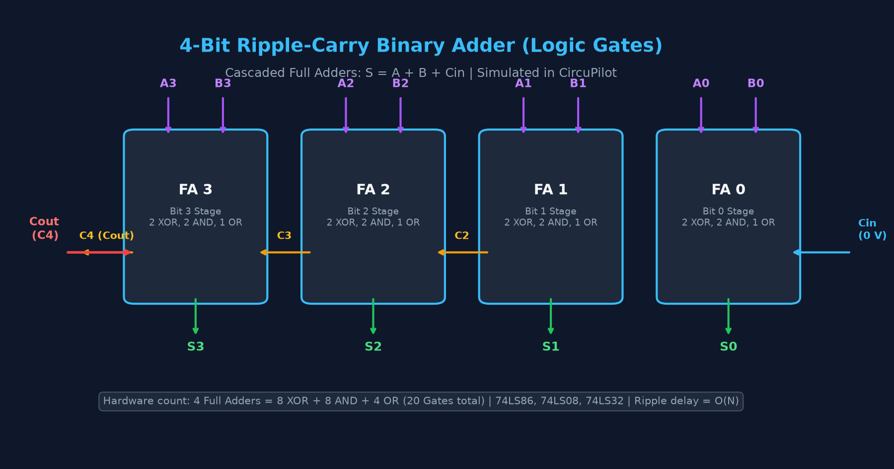
When planning the gate-level schematic, two design variants exist:
1. The 20-Gate Architecture (4 Full Adders): Every stage, including Bit 0 (FA0), is a complete full adder (5 gates × 4 = 20 logic gates). This preserves an explicit Cin input on Bit 0. This architecture is essential if you want to cascade multiple 4-bit adders into 8-bit or 16-bit units, or implement two's complement subtraction (A - B = A + ~B + 1) by setting Cin = 1.
2. The 17-Gate Architecture (1 Half Adder + 3 Full Adders): If Bit 0 never receives a carry-in (Cin = 0), FA0 simplifies to a 2-gate Half Adder (1 XOR, 1 AND), eliminating 1 XOR, 1 AND, and 1 OR gate (2 + 15 = 17 logic gates).
Implementation note: The interactive 4-bit simulation link provided below uses the 20-gate architecture (4 Full Adders) with an interactive Logic Toggle on Cin. This allows you to toggle Cin directly on the canvas and observe how incoming carries affect the entire chain in real-time.
              A3   B3              A2   B2              A1   B1              A0   B0
               |    |               |    |               |    |               |    |
               v    v               v    v               v    v               v    v
            +-----------+        +-----------+        +-----------+        +-----------+
  Cout <----+  FA 3     |<--C3---+  FA 2     |<--C2---+  FA 1     |<--C1---+  FA 0     |<-- Cin (0 V)
 (C4)       +-----+-----+        +-----+-----+        +-----+-----+        +-----+-----+
                  |                    |                    |                    |
                  v                    v                    v                    v
                  S3                   S2                   S1                   S0
4. Hardware Implementation: The 74xx IC Reality
In university laboratory sessions, instructors frequently require students to wire a 4-bit adder using discrete logic gates on a breadboard before introducing single-chip adders.
Let's calculate the component count required for the 20-gate implementation:
- XOR gates: 2 per full adder × 4 stages = 8 gates
- AND gates: 2 per full adder × 4 stages = 8 gates
- OR gates: 1 per full adder × 4 stages = 4 gates
- Total logic gates: 20 gates
To implement this on a breadboard using standard 74xx DIP chips:
| IC Part Number | Logic Type | Gates per Chip | Chips Needed for 4-Bit Adder |
|---|---|---|---|
| 74LS86 / 74HC86 | Quad 2-Input XOR | 4 gates | 2 chips (8 gates used) |
| 74LS08 / 74HC08 | Quad 2-Input AND | 4 gates | 2 chips (8 gates used) |
| 74LS32 / 74HC32 | Quad 2-Input OR | 4 gates | 1 chip (4 gates used) |
Wiring 20 gates across 5 physical 14-pin ICs requires over 40 jumper wires between gates, plus VCC and GND connections to each IC. A single misplaced jumper wire on Bit 1 corrupts all subsequent higher-order sum bits.
Because of this wiring density, integrated circuit manufacturers introduced dedicated 4-bit binary full adders in a single 16-pin package: the 74LS83 and 74LS283. Internally, they implement the exact same Boolean addition, but utilize fast internal lookahead carry generation inside the silicon.
5. Simulating the 4-Bit Adder in CircuPilot
In CircuPilot, you can simulate the complete 20-gate discrete circuit interactively and verify that every bit voltage matches the theoretical truth table.
Measured ngspice Node Voltages for Individual Bits
The table below records the simulated steady-state DC operating point voltages for all five output lines (S3, S2, S1, S0, and Cout) across 7 test cases:
| Test Case | Operand A | Operand B | V(S3) [Bit 3] | V(S2) [Bit 2] | V(S1) [Bit 1] | V(S0) [Bit 0] | V(Cout) [Carry] | Result [S3..S0] |
|---|---|---|---|---|---|---|---|---|
| Zero addition | 0 (0000₂) | 0 (0000₂) | 0.00 V (0) | 0.00 V (0) | 0.00 V (0) | 0.00 V (0) | 0.00 V (0) | 0000₂ (0) |
| Single-bit addition | 1 (0001₂) | 2 (0010₂) | 0.00 V (0) | 0.00 V (0) | 4.95 V (1) | 4.95 V (1) | 0.00 V (0) | 0011₂ (3) |
| Mid-range addition | 5 (0101₂) | 3 (0011₂) | 4.95 V (1) | 0.00 V (0) | 0.00 V (0) | 0.00 V (0) | 0.00 V (0) | 1000₂ (8) |
| Carry ripple across 3 bits | 7 (0111₂) | 1 (0001₂) | 4.95 V (1) | 0.00 V (0) | 0.00 V (0) | 0.00 V (0) | 0.00 V (0) | 1000₂ (8) |
| Maximum 4-bit sum | 9 (1001₂) | 6 (0110₂) | 4.95 V (1) | 4.95 V (1) | 4.95 V (1) | 4.95 V (1) | 0.00 V (0) | 1111₂ (15) |
| Full 4-bit overflow | 15 (1111₂) | 1 (0001₂) | 0.00 V (0) | 0.00 V (0) | 0.00 V (0) | 0.00 V (0) | 4.94 V (1) | 0000₂ (0, Cout=1) |
| Max operands overflow | 15 (1111₂) | 15 (1111₂) | 4.95 V (1) | 4.95 V (1) | 4.95 V (1) | 0.00 V (0) | 4.94 V (1) | 1110₂ (14, Cout=1) |
Open the interactive 4-bit Binary Adder in CircuPilot →
6. Understanding Overflow: Unsigned Carry vs Signed Overflow
In unsigned 4-bit arithmetic, numbers span from 0 to 15 (0000₂ to 1111₂). When adding 15 (1111₂) and 1 (0001₂), the true sum is 16 (10000₂). Because the sum register holds only 4 bits, the result wraps around (sum modulo 16) to 0000₂, and the Carry-out (Cout / C4) line transitions to 4.94 V (Logic HIGH), serving as the 16s column.
Unsigned Carry vs Signed Two's Complement Overflow
It is important not to confuse Carry-out (Cout) with Signed Overflow (V):
- Unsigned Carry (
Cout): Indicates that the unsigned sum exceeded the maximum 4-bit range (15). In microcontrollers like the AVR ATmega328P, this sets the Carry (C) flag in the Status Register (SREG). - Signed Overflow (
Vflag): In signed two's complement representation, 4 bits represent values from -8 to +7, where Bit 3 is the sign bit. Signed overflow occurs when adding two numbers of the same sign produces a result with the opposite sign (e.g.,+5 + +4 = -7). The processor detects this condition using the logic conditionV = C3 ⊕ C4(whereC3is the carry entering the sign bit andC4is the carry leaving it).
This adder circuit implements pure unsigned arithmetic; Cout represents the 5th magnitude bit.
7. Interactive Logic Toggles and Logic Probes
In CircuPilot, you do not need to wire separate DC power supplies, ground switches, or discrete pull-down resistors to test digital logic. Under the Digital Logic category in the component palette, CircuPilot provides two dedicated interactive components:
1. Logic Toggle (Logic Input): An interactive digital switch placed directly on the schematic. Clicking it on the canvas flips its state between 0 (0 V) and 1 (5 V). Every click automatically triggers immediate real-time DC simulation without requiring you to manually restart the simulator.
2. Logic Probe (Logic Output): A compact digital indicator box that connects to any node and displays a red 1 (for voltages above 2.5 V) or a blue 0 (for voltages below 2.5 V). Under the hood, the probe transparently provides a high-impedance 10 MΩ DC path to ground in SPICE, ensuring topological closure and preventing open-circuit errors.
The interactive simulation links for the 1-bit Full Adder and the 4-bit Binary Adder are pre-wired using these exact Logic Toggles and Logic Probes. You can click on any input bit (A0–A3 or B0–B3) and watch the Sum and Carry probes update instantly.
8. Carry Propagation Delay in Physical Hardware
While the ripple-carry topology is conceptually simple, physical hardware encounters a fundamental speed barrier: propagation delay (tpd).
In standard 74HC CMOS logic operating at 5 V, typical datasheet propagation delay values range between approximately 9 ns and 15 ns per gate:
- Sum Bit 0 (
S0) is ready after 2 XOR gate delays (~20 ns). - Carry Bit 1 (
C1) requires 1 XOR delay + 1 AND delay + 1 OR delay (~30 ns). - Stage 1 cannot compute its final Sum (
S1) and carry (C2) untilC1arrives. - Stage 2 must wait for
C2. - Stage 3 must wait for
C3.
For an N-bit ripple-carry adder, the worst-case carry propagation delay scales linearly: t_worst = O(N).
In digital simulation, the DC operating point captures the resolved arithmetic output once all logic paths stabilize. In physical hardware, the carry propagation delay represents the brief nanosecond interval required for internal signals to settle into this exact equilibrium.
In 32-bit and 64-bit microprocessors, waiting for a carry bit to ripple sequentially across 32 or 64 stages would severely restrict the maximum clock frequency of the arithmetic logic unit (ALU). Modern high-performance CPUs therefore implement Carry-Lookahead Adders (CLA) or parallel prefix trees (such as Kogge-Stone or Brent-Kung adders), which compute generate (G = A · B) and propagate (P = A ⊕ B) terms in parallel using logarithmic depth O(log N).
Summary & Next Steps
Constructing a 4-bit binary adder demonstrates how arithmetic logic emerges from fundamental Boolean gates:
- A Half Adder adds two bits (
XORfor Sum,ANDfor Carry). - A Full Adder adds three bits by combining two Half Adders and an
ORgate. - Four cascaded Full Adders form a complete 4-bit ripple-carry unit capable of adding numbers from 0 to 15 with carry overflow detection.
- Real-world digital architectures trade the wiring simplicity of ripple-carry adders for the parallel speed of carry-lookahead logic.
You can experiment with logic gates and verify truth tables directly in your browser without installing software. Explore our logic gate simulation tutorial or test custom circuits on the CircuPilot simulator.
Frequently asked questions
How many logic gates are needed to build a 4-bit binary adder?
A standard 4-bit ripple-carry adder built from discrete gates requires 20 logic gates (8 XOR, 8 AND, 4 OR) when all four stages are full adders. If bit 0 does not require an incoming carry, it can use a half adder, reducing the total to 17 gates (7 XOR, 7 AND, 3 OR).
What is the difference between a half adder and a full adder?
A half adder adds only two 1-bit inputs (A and B) and produces a Sum and Carry. It cannot accept an incoming carry from a previous stage. A full adder accepts three 1-bit inputs (A, B, and Cin), allowing it to be cascaded into multi-bit addition circuits.
Why is it called a ripple-carry adder?
It is named a ripple-carry adder because the carry-out generated at each bit position ripples sequentially through each successive stage from the least significant bit (LSB) to the most significant bit (MSB) before the final sum bits stabilize.
Which 74xx IC chips are required to build a 4-bit adder on a breadboard?
To wire a 4-bit adder from basic gates on a breadboard, you need 5 integrated circuits: two 74LS86 (Quad XOR), two 74LS08 (Quad AND), and one 74LS32 (Quad OR). Alternatively, you can use a single 74LS283 or 74LS83 IC, which integrates a complete 4-bit binary full adder with lookahead carry into one 16-pin chip.
Why do digital circuits in CircuPilot use Logic Probes and Logic Toggles?
Logic Toggles allow users to flip digital inputs between 0 and 1 directly on the canvas with a single click. Logic Probes display resolved 0 and 1 bit states while internally providing a 10 MΩ DC path to ground in SPICE, eliminating the need to wire separate discrete pull-down resistors to prevent floating terminal nodes.