
A voltage regulator maintains a steady DC output voltage regardless of changes in the unregulated input voltage or variations in load current. The simplest shunt regulator consists of just two discrete components: a current-limiting series resistor and a Zener diode.
While modern electronic systems commonly use three-terminal integrated regulators (such as the LM7805 or adjustable buck converters), Zener shunt regulators remain ubiquitous for analog reference voltages, microcontroller ADC clamping, sensor biasing, and low-current auxiliary rails.
In this guide, we examine the physics behind Zener regulation, derive the exact design equations for the series resistor, simulate a 5.1V regulator circuit using SPICE, analyze why dynamic impedance prevents an entirely flat output, and investigate why the regulated voltage collapses when overloaded.
You can launch and interact with the verified pre-wired circuit directly in your browser:
---
1. What Is a Zener Diode Voltage Regulator?
A standard rectifier diode (such as a 1N4007) conducts current easily when forward-biased (anode positive relative to cathode) with a forward voltage drop of approximately 0.7 V. In the reverse direction, it blocks current until reaching its peak inverse voltage (PIV), at which point destructive breakdown occurs.
A Zener diode is deliberately manufactured with controlled, heavy semiconductor doping to exhibit a sharp, non-destructive reverse breakdown knee at a precisely specified voltage, known as the Zener voltage (Vz).
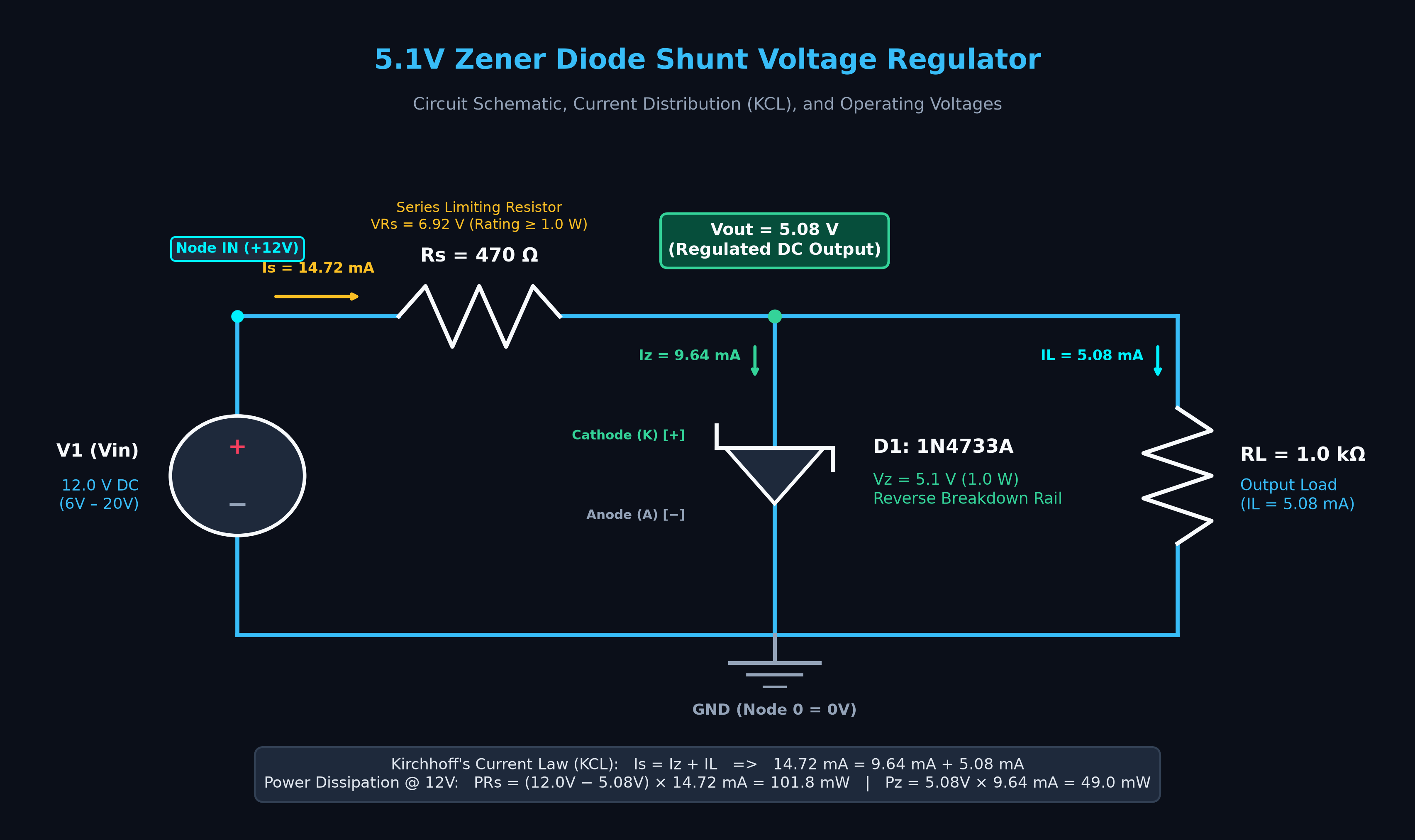
When connected in reverse bias across a load (cathode connected to the positive supply rail and anode connected to ground), the Zener diode holds the voltage across its terminals nearly constant over a range of reverse currents. The series resistor absorbs the voltage difference between the higher input supply and the regulated output.
---
2. How Does a Zener Regulator Work?
To understand how the circuit stabilizes voltage, consider Kirchhoff's Current Law (KCL) at the output node (OUT):
I_s = I_z + I_L
Where:
I_sis the total current flowing from the unregulated source through the series resistorR_s.I_zis the reverse current passing through the Zener diode.I_Lis the load current drawn by the downstream circuit (I_L = V_out / R_L).
The voltage drop across the series resistor is determined by Ohm's law:
V_Rs = V_in - V_out
I_s = (V_in - V_out) / R_s
The Self-Balancing Mechanism
The Zener diode acts as an automatic variable current sink that dynamically compensates for fluctuations:
1. If the input voltage (V_in) rises: The total supply current I_s increases. Because the load resistance R_L is fixed, it demands roughly I_L = V_z / R_L. The Zener diode absorbs the excess current (I_z increases). The increased current through R_s increases the voltage drop across R_s, keeping V_out close to V_z.
2. If the load current (I_L) increases (load resistance drops): The load demands more current. The Zener diode releases current by reducing its own conduction (I_z decreases) so that total current I_s remains virtually constant. As long as I_z stays above the knee holding current, regulation holds.
Why the Regulated Output Is Not Perfectly Constant (Dynamic Impedance)
In an ideal theoretical model, a Zener diode maintains an absolutely flat, horizontal voltage curve in breakdown. In reality, every physical Zener diode possesses an internal non-zero dynamic impedance (or slope resistance, Zz):
Z_z = ΔV_z / ΔI_z
As input voltage increases, more current flows through the Zener diode. This incremental current ΔI_z multiplied by Z_z produces a slight positive voltage rise:
V_z(actual) ≈ V_z0 + (I_z · Z_z)
This explains why measured line regulation curves exhibit a slight positive slope rather than a perfectly flat horizontal line.
---
3. How to Calculate the Series Resistor (R_s)
Choosing the series resistor requires balancing two competing extremes:
- Condition A (Minimum Input & Maximum Load): If
R_sis too large, the voltage drop across it will be excessive, starving the Zener diode of current and causing the output voltage to sag under load. - Condition B (Maximum Input & No Load): If
R_sis too small, excessive current will flow through the Zener diode and resistor when the load is disconnected, overheating and destroying the components.
Design Formula
To guarantee that regulation never drops out under worst-case operating conditions, calculate R_s at the minimum input voltage and maximum load current:
R_s = (V_in(min) - V_z) / (I_L(max) + I_z(min))
Where:
V_in(min)is the lowest expected DC input supply voltage.V_zis the nominal Zener diode breakdown voltage.I_L(max)is the maximum current drawn by the load (V_z / R_L(min)).I_z(min)is a chosen design assumption for minimum holding current.
Understanding Knee Current from Datasheets vs. Design Assumptions
In manufacturer datasheets for the 1N4733A (e.g., Vishay or ON Semiconductor):
- The nominal breakdown voltage
V_z = 5.1 V(±5% tolerance) is specified at a heavy nominal test current ofI_ZT = 49 mA, where dynamic impedance is low (Z_ZT ≤ 7 Ω). - The datasheet also defines a reverse knee current
I_ZK = 1.0 mA, where dynamic impedance increases substantially (Z_ZK ≤ 1000 Ω).
Operating right at I_ZK = 1 mA is risky because small load disturbances can drop the diode out of breakdown. However, operating at the full 49 mA test current causes high power dissipation and poor efficiency.
Therefore, for this practical design example, we select I_z(min) = 3 mA as a design assumption—an engineering compromise that keeps the diode reliably above the high-impedance knee (I_ZK = 1.0 mA) without drawing unnecessary quiescent current.
Numerical Example
Suppose our unregulated DC supply fluctuates between 9 V and 15 V (with occasional transient excursions up to 20 V). The load demands up to 5 mA (R_L(min) = 1 kΩ). We select a nominal 5.1V Zener diode and set our design assumption I_z(min) = 3 mA:
R_s = (9.0 V - 5.1 V) / (5.0 mA + 3.0 mA) = 3.9 V / 8.0 mA = 487.5 Ω
Selecting the closest standard E24 5% resistor yields 470 Ω.
At nominal 12 V input with R_s = 470 Ω:
I_s = (12.0 V - 5.08 V) / 470 Ω = 14.72 mA
I_L = 5.08 V / 1000 Ω = 5.08 mA
I_z = 14.72 mA - 5.08 mA = 9.64 mA
The Zener current of 9.64 mA comfortably exceeds our 3 mA design margin.
---
4. SPICE Simulation and Behavioral Model Context
We simulate this circuit in CircuPilot using ngspice to measure operating point voltages, currents, and power dissipation.
The SPICE Behavioral Model
In our simulation catalog, the 1N4733A is represented by the standard SPICE diode model:
.model 1N4733A D(Is=1.5n Rs=1.5 N=1.7 Cjo=200p M=.35 tt=1n Bv=5.1 Ibv=20m)Engineering Context on SPICE Models: This model is a first-order behavioral macromodel using standard SPICE diode junction equations. It specifies a breakdown voltage
Bv = 5.1 Vat reverse breakdown currentIbv = 20 mAwith internal series bulk resistanceRs = 1.5 Ω. While it reliably simulates qualitative breakdown dynamics, line regulation slope, and load dropout for educational and engineering design purposes, it is a simplified behavioral approximation rather than a physical part reproduction containing production batch tolerances (±5%) or temperature drift coefficients.
SPICE Netlist
* 5.1V Zener Diode Shunt Voltage Regulator
V1 IN 0 12V
R1 IN OUT 470
D1 0 OUT 1N4733A
RL OUT 0 1k
.model 1N4733A D(Is=1.5n Rs=1.5 N=1.7 Cjo=200p M=.35 tt=1n Bv=5.1 Ibv=20m)
.end
Measured DC Operating Point (Vin = 12V, RL = 1 kΩ)
| Parameter | Theoretical First-Order | SPICE Simulation Result | Status / Notes |
|---|---|---|---|
Input Voltage (V_in) | 12.000 V | 12.000 V | Applied DC Rail |
Output Voltage (V_out) | 5.100 V | 5.0826 V | Behavioral Model Equilibrium |
Total Supply Current (I_s) | 14.68 mA | 14.72 mA | Confirmed by Ohm's Law |
Load Current (I_L) | 5.10 mA | 5.08 mA | Confirmed through 1 kΩ load |
Zener Diode Current (I_z) | 9.58 mA | 9.64 mA | Active Reverse Breakdown |
Zener Power Dissipation (P_z) | 48.86 mW | 48.97 mW | Safe (< 1.0 W rating) |
Series Resistor Power (P_Rs) | 101.3 mW | 101.81 mW | Safe (< 0.5 W rating) |
The simulated output of 5.0826 V reflects the diode conduction equilibrium in ngspice with Rs = 1.5 Ω at ~9.6 mA.
---
5. Line Regulation: Input Voltage Sweep (6 V to 20 V)
Line regulation measures the regulator's ability to maintain a steady output when the input supply voltage fluctuates.
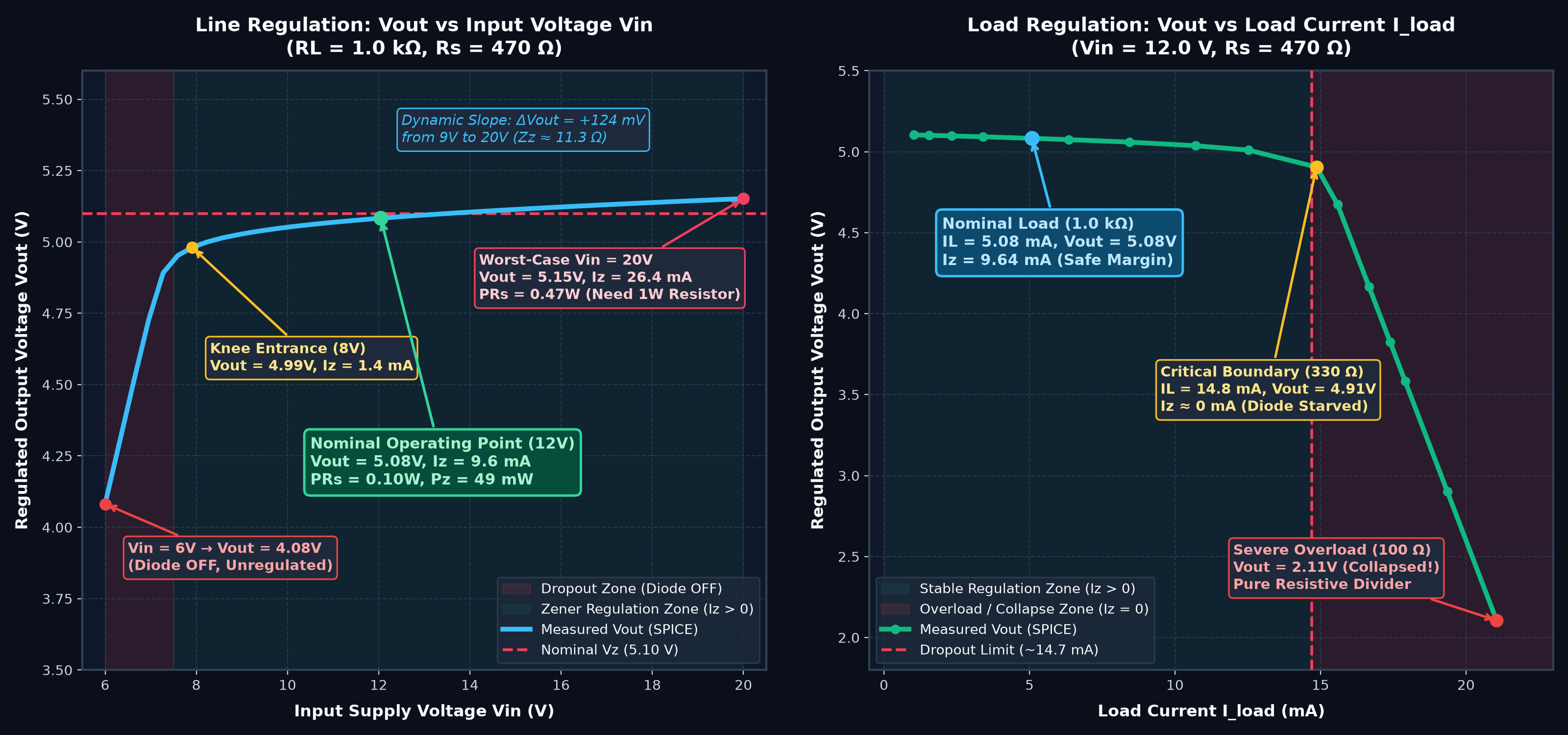
We simulated an input voltage sweep across the complete range from 6.0 V to 20.0 V in ngspice with R_L = 1 kΩ and R_s = 470 Ω.
Simulated Line Regulation Data (Full Sweep 6.0 V to 20.0 V)
| Input Voltage (Vin) | Output Voltage (Vout) | Supply Current (Is) | Load Current (IL) | Zener Current (Iz) | Zener Power (Pz) | Resistor Power (PRs) | Operating Status |
|---|---|---|---|---|---|---|---|
| 6.0 V | 4.0816 V | 4.08 mA | 4.08 mA | 0.00 mA | 0.00 mW | 7.83 mW | Unregulated (Diode OFF) |
| 8.0 V | 4.9867 V | 6.41 mA | 4.99 mA | 1.42 mA | 7.10 mW | 19.32 mW | Entering Knee Region |
| 9.0 V | 5.0280 V | 8.45 mA | 5.03 mA | 3.42 mA | 17.21 mW | 33.57 mW | Regulated (Design Min) |
| 10.0 V | 5.0517 V | 10.53 mA | 5.05 mA | 5.48 mA | 27.67 mW | 52.10 mW | Fully Regulated |
| 12.0 V | 5.0826 V | 14.72 mA | 5.08 mA | 9.64 mA | 48.97 mW | 101.81 mW | Nominal Operating Point |
| 15.0 V | 5.1139 V | 21.03 mA | 5.11 mA | 15.92 mA | 81.42 mW | 207.95 mW | Fully Regulated |
| 18.0 V | 5.1380 V | 27.37 mA | 5.14 mA | 22.23 mA | 114.21 mW | 351.98 mW | Fully Regulated |
| 20.0 V | 5.1519 V | 31.59 mA | 5.15 mA | 26.44 mA | 136.22 mW | 469.08 mW | Regulated (Max Voltage Stress) |
Across the entire regulated operating span between 9.0 V and 20.0 V (an 11.0 V or 122% input increase), the output voltage changes by only 0.1239 V (123.9 mV):
Line Regulation = ΔV_out / ΔV_in = (5.1519 V - 5.0280 V) / (20.0 V - 9.0 V) = 123.9 mV / 11.0 V = 11.26 mV/V
This 11.26 mV/V slope directly illustrates the effect of the diode internal dynamic impedance modeled in SPICE.
---
6. Load Regulation: Why Does Zener Diode Voltage Drop Under Load?
A frequent issue encountered when testing Zener regulators is observing the regulated output voltage sag significantly below V_z once a heavy load is connected.
The Breakdown Dropout Mechanism
The maximum total current the series resistor can supply before output voltage drops below breakdown is limited by the available input voltage:
I_s(max) ≈ (V_in - V_z) / R_s
For our nominal 12 V input with R_s = 470 Ω:
I_s(max) ≈ (12.0 V - 5.1 V) / 470 Ω = 14.68 mA
If the load resistance R_L is made too small and attempts to draw more than ~14.7 mA, the Zener diode current drops to zero (I_z = 0). The diode leaves reverse breakdown and shuts off completely.
Once the Zener diode turns off, the circuit stops functioning as a regulator and collapses into a passive resistive voltage divider:
V_out = V_in · (R_L / (R_s + R_L))
Simulated Load Regulation Data (Vin = 12V, Rs = 470 Ω)
| Load Resistance (RL) | Output Voltage (Vout) | Supply Current (Is) | Load Current (IL) | Zener Current (Iz) | Zener Power (Pz) | Operating Mode |
|---|---|---|---|---|---|---|
| 1 MΩ (No Load) | 5.1084 V | 14.66 mA | 0.01 mA | 14.66 mA | 74.88 mW | Regulated (Max No-Load Zener Power) |
| 5.0 kΩ | 5.1038 V | 14.67 mA | 1.02 mA | 13.65 mA | 69.68 mW | Regulated |
| 2.2 kΩ | 5.0976 V | 14.69 mA | 2.32 mA | 12.37 mA | 63.05 mW | Regulated |
| 1.0 kΩ | 5.0826 V | 14.72 mA | 5.08 mA | 9.64 mA | 48.97 mW | Nominal Operating Point |
| 470 Ω | 5.0369 V | 14.82 mA | 10.72 mA | 4.10 mA | 20.64 mW | Regulated (Near Knee Margin) |
| 330 Ω | 4.9054 V | 15.09 mA | 14.86 mA | 0.23 mA | 1.13 mW | Transition / Dropout Boundary |
| 220 Ω | 3.8261 V | 17.39 mA | 17.39 mA | 0.00 mA | 0.00 mW | Dropout: Voltage Divider (12 · 220/690) |
| 100 Ω | 2.1053 V | 21.05 mA | 21.05 mA | 0.00 mA | 0.00 mW | Dropout: Voltage Divider (12 · 100/570) |
As shown in the right plot of Figure 2, when R_L drops to 220 Ω, the required current exceeds 14.7 mA. The Zener diode turns off (I_z = 0.00 mA), and the output voltage sags to exactly 3.8261 V—matching the voltage divider formula 12 V · (220 / (470 + 220)).
---
7. Power Dissipation and Critical Resistor Sizing at 20 V
A critical engineering failure in shunt regulators is selecting an undersized series resistor wattage.
Worst-Case Analysis: 20 V Input with No Load Connected
The absolute worst-case power dissipation for both the Zener diode and the series resistor occurs at maximum input voltage (V_in = 20 V) when the load is completely disconnected (R_L = ∞):
1. Simulated Output Voltage: V_out = 5.1673 V
2. Current through Resistor and Zener:
I_s = I_z = (20.0 V - 5.1673 V) / 470 Ω = 31.56 mA
3. Worst-Case Zener Power Dissipation:
P_z(max) = 5.1673 V · 31.56 mA = 163.08 mW (0.163 W)
Since the 1N4733A diode is rated for 1.0 W (1000 mW), 163 mW is well within its safe operating area (~16% of capacity).
4. Worst-Case Series Resistor Power Dissipation:
P_Rs(max) = I_s² · R_s = (31.56 mA)² · 470 Ω = 468.10 mW (0.468 W)
The 1/2W vs. 1W Resistor Trap
Notice that under maximum 20 V input conditions, the power dissipated in R_s reaches 0.468 W (almost 0.47 W):
- A standard 1/2-watt (0.50 W) resistor would operate at 94% of its absolute maximum rating. In an enclosed chassis or at elevated ambient temperature, a resistor operating at 94% capacity will exceed 100°C, drift in resistance, scorch the circuit board, and eventually fail open-circuit.
- Engineering Recommendation: If the circuit must withstand sustained 20 V input without load, you must use a resistor rated for at least 1.0 W (or two 1/2W 240 Ω resistors in series) to provide an adequate 50% derating safety margin.
- If the maximum input voltage is constrained to 15 V,
P_Rs(max)drops to 0.208 W, in which case a 1/2-watt resistor operates with a safe 60% derating margin.
---
8. Common Design Mistakes and How to Avoid Them
1. Reversing Zener Diode Polarity: Connecting the diode in forward bias (anode to positive rail) turns it into a standard silicon rectifier diode, clamping the output to only 0.7 V instead of 5.1 V. The cathode band must face the positive voltage rail.
2. Using a 1/4W or 1/2W Resistor at High Inputs: As proven by our 20 V calculation above, R_s dissipates significant heat when the load is disconnected. Always verify P_Rs = (V_in(max) - V_z)² / R_s and select a 1W or higher rated power resistor.
3. Omitting the Knee Current Margin: Calculating R_s assuming I_z = 0 at maximum load current leaves zero margin. The slightest load increase drops the diode out of breakdown.
4. Expecting Zero Line Variation: Because physical Zener diodes have dynamic impedance (Z_z), the output will always rise slightly with higher input voltages. For precision instrumentation requiring microvolt stability, use a bandgap reference (such as an LM336, TL431, or REF02).
5. Excessive Heat in High-Current Loads: Shunt regulators draw full supply current continuously, dissipating significant energy as heat even when the load is idle. For load currents exceeding 50 mA, use an active linear regulator (e.g. LM7805 or LM317) or a switching buck converter.
---
9. Interactive Simulation in CircuPilot
You can inspect, probe, and experiment with this exact 5.1V Zener regulator circuit directly in your browser:
1. Open the Pre-wired 5.1V Zener Diode Voltage Regulator in CircuPilot.
2. Click Run to view live node voltages and current flows computed by real SPICE simulation.
3. Double-click the voltage source V1 to change input voltage from 12 V to 20 V or 9 V, and verify how V_out remains within the 5.03V to 5.15V window.
4. Decrease RL from 1 kΩ to 220 Ω to witness the load regulation dropout knee in real time.
If you are designing power and filtering stages, explore our companion guides on Full-Wave Bridge Rectifiers with Capacitor Filters and RC Time Constant Charge & Decay Simulation.
Frequently asked questions
How do I calculate a Zener regulator resistor?
Calculate the series resistor using the minimum expected input voltage and maximum expected load current: Rs = (Vin(min) - Vz) / (IL(max) + Iz(min)). Here, Vz is nominal Zener voltage, IL(max) is peak load current, and Iz(min) is a chosen design assumption (typically selected between 1 mA and 5 mA in low-current designs) to keep the diode safely above its knee current.
Why does my Zener diode voltage drop under load?
If load current exceeds the current supplied through the series resistor (IL > (Vin - Vz) / Rs), the Zener diode current drops to zero. The diode leaves the reverse breakdown region and turns off completely. At that point, the circuit stops regulating and collapses into an unbuffered resistive voltage divider formed by Rs and RL, causing the output voltage to sag severely below Vz.
Why does the output voltage change slightly when input voltage changes?
A Zener diode is not an ideal zero-impedance voltage source. In reverse breakdown, it possesses a non-zero dynamic impedance (Zz = ΔVz / ΔIz). As input voltage increases, additional current flows through the Zener, producing an incremental voltage drop across Zz that causes the regulated output to rise slightly with higher inputs.
How much power does a Zener diode and its series resistor dissipate?
Maximum Zener power dissipation occurs under no-load conditions (RL disconnected), where all supply current flows through the diode: Pz(max) = Vz · (Vin(max) - Vz) / Rs. Similarly, worst-case power in the series resistor occurs at maximum input without load: PRs(max) = (Vin(max) - Vz)² / Rs. At Vin = 20V with Rs = 470 Ω, PRs reaches approximately 0.47W, requiring a 1W rated resistor rather than a 1/2W component.
What is the difference between manufacturer datasheet ratings and standard SPICE diode models?
Manufacturer datasheets (such as Vishay or ON Semiconductor for 1N4733A) specify nominal breakdown Vz = 5.1V ±5% at a heavy test current IZT = 49 mA with dynamic impedance ZZT ≤ 7 Ω, and a knee current IZK = 1.0 mA with ZZK ≤ 1000 Ω. Standard SPICE diode behavioral models approximate this behavior using model parameters (such as Bv = 5.1V at Ibv = 20 mA with internal series resistance Rs = 1.5 Ω). They provide reliable qualitative and circuit-level behavior but are behavioral macromodels rather than exact empirical representations of all device variations.